

Printed circuit boards (PCBs) are an indispensable component of modern electronic devices. They are used to connect various electronic components for products such as mobile phones, laptops, computers, and other consumer electronics, including game consoles and smart home devices. As boards become increasingly complex in their layout, the value of the electronic components and chips used on the board has increased. Identification of the board is essential to ensure authenticity, traceability, and identification, but what process should manufacturers be using? By using the right process, manufacturers can protect their products from knock-offs, add identification traceability, and ensure that consumers receive safe and functioning products.
Laser marking vs. PCB labeling: what is the difference?
Traditionally, in PCB assembly, applying labels to boards is a manual task to identify the original intended use or even to define the version of the board being produced. Label application is very time-consuming and can be error-prone if manually carried out. However, since PCB labels are tiny in size and hard to handle. Finding a machine to handle this operation can be challenging. Moreover, even if a machine could apply these labels, they would not be secure forever, as they could fall off over time, get scratched, experience ink fade, or simply fall off the board. In contrast, laser marking modules are able to accurately scan and locate the positions where the laser should mark and override durability issues since the information is laser-etched directly onto the PCB itself. This method offers several benefits over traditional labeling, including increased accuracy, improved efficiency, and reduced errors.
By replacing labeling with laser marking, manufacturers can streamline the assembly process, reduce production time, and improve the quality of their products. But let’s take a closer look at the benefits.
Increased automation and efficiency
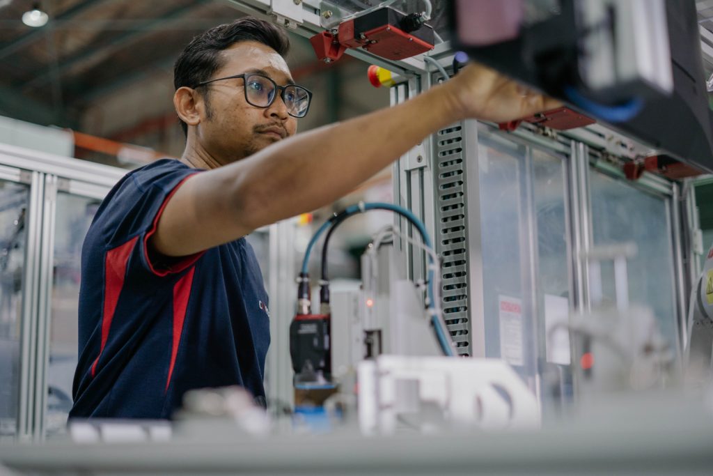
One of the most significant factors in any production is to increase throughput and optimize processes to improve production efficiency. Instead of creating a bottleneck with a manual workstation and operator, or worse, unloading stacks of boards to be manually labeled, adding automation such as a laser marker brings a lot of value to the board assembly process.
How Laser Markers Work
Laser markers are designed to only etch the surface of a board, not burn holes through it. Reputable manufacturers offering laser marking modules should provide sample markings for your review and testing.
Technically speaking, a laser beam is directed across the surface of the circuit board, and the reflection is captured by a sensor. The data obtained from the reflection is then used to create an accurate 3D circuit board map. This technology can measure to an accuracy of a few micrometers, allowing for a level of precision that is impossible with manual labeling. This increased accuracy is crucial in ensuring the circuit board is correctly marked and completed with visual inspection cameras.
Improved traceability & serialization
An advanced laser marker system can be connected to a company’s EMS system, which then can provide serial numbers to allow for serialization and full traceability of a PCB. This meets the safety and security needs of industries requiring a higher data granularity, such as defense, medical devices, and automotive, to name a few. In fact, many companies in these industries are opting for laser marking solutions due to their increased reliability compared to manual labeling.
Better quality control
The manufacturer should provide software and a user-friendly interface to allow you to store barcodes, auto-serialize, create 2D barcodes, or even upload a company logo for marking. Your vendor should offer a range of tools, from human-readable markings to standard barcode types, to facilitate a quick start.
Overall, incorporating laser marking technology in PCB assembly is a practical and effective solution for improving production processes’ efficiency, speed, and quality. It provides the ability to identify and tracking boards while eliminating manual processes. The reliability and consistency of laser marking enhance the quality of boards produced, making it a preferred option for manufacturers assembling PCBs and for their customers.
Visit us at productronica 2023 and learn more about efficient PCB handling!
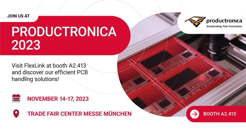
Are you keen to learn more about PCB handling? Then visit us at productronica 2023 in Munich at booth A2.413 from November 14-17. You can secure your ticket and schedule a personal meeting with our team of experts via our contact form. Our team looks forward to discussing your PCB handling needs with you!
Learn more about FlexLink in our blog section or follow us on LinkedIn here.


Leave a Reply